
BD86852MUF-C
車電用相機電源管理IC
BD86852MUF-C
車電用相機電源管理IC
Quick Download
Description
BD86852MUF-C是針對CMOS影像感測器的電源供應所設計之電源管理IC,內含主降壓型DC-DC轉換器(DC/DC1),第二級降壓型DC-DC轉換器(DC/DC2和DC/DC3)、外部線性穩壓器控制區塊以及電源重置功能。其輸出電壓及順序可供選擇,並適用於多種影像感測器的電源供應。本產品採用VQFN24FV4040小型封裝,最適用於相機模組。此外,此裝置具有一個可編程引腳,用於開啟/關閉展頻,從而提供較低雜訊的穩壓輸出。 A Product Change Notice (PCN) is scheduled for this product.
While there will be no changes to electrical characteristics, certain specifications will be updated.
If you would like evaluation samples, please contact your sales representative or use the "Contact Us" form.
Product Detail
Specifications
ch
3
Vin1(Min.)[V]
4
Vin1(Max.)[V]
18
Output Voltage1 (Min.)[V]
3.3
Output Voltage1 (Max.)[V]
3.9
Output Current Capacity 1 [A]
2
Output Voltage2 (Min.)[V]
1.1
Output Voltage2 (Max.)[V]
1.2
Output Current Capacity 2 [A]
1
SW frequency(Max.)[MHz]
2.2
Circuit Current(Typ.)[mA]
3
Operating Temperature (Min.)[°C]
-40
Operating Temperature (Max.)[°C]
125
Package Size [mm]
4.0x4.0 (t=1.0)
Common Standard
AEC-Q100 (Automotive Grade)
Features
- AEC-Q100 合格產品 (Grade 1)
- 輸出電壓:
VO1: 3.3V 或 3.9V (±2%)
VO2: 1.1V 或 1.2V (±2%)
VO3: 1.8V (±2%) - 輸出電流:
VO1: 2A (最大)
VO2: 1A (最大)
VO3: 1A (最大) - 功能安全支援車用產品
- 主DC/DC (VO1)
內建FET之DC/DC
高效率同步整流 - 雙第二級DC/DC (VO2, VO3)
內建FET之DC/DC
高效率同步整流 - 各種保護功能
- 展頻 (Spread Spectrum) 可改善電磁相容性(EMC)
- 故障偵測腳位(用於各個輸出)
- 輸出電壓和時序可選擇
Reference Design / Evaluation Tool
-
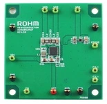
- Evaluation Board - BD86852-TSB-001
BD86852-TSB-001 is an evaluation board for Power Management IC BD86852MUF-C that is suitable for Camera module application such as ADAS camera sensor. BD86852MUF-C integrate primary buck converter (DC/DC1), secondary buck converters (DC/DC2 and DC/DC3). Together with on board linear regulator, all power rails required for CMOS image sensor and image processor are available. The PCB layout has been miniaturized and optimized for use in camera modules.
